Point-to-point optical wireless network for factory communications
Author: Luís Botelho Ribeiro
Address: LUSOPTEL L.da, R. Dr. José Correia, 79, 4580 Paredes, Portugal
Telef: 055-777428
Fax: 034-381128
Email: botelho@relay.ua.pt
Point-to-point optical wireless network for factory communications
Author: Luís Botelho Ribeiro
Submission area: Factory Automation
Abstract: An exploratory network has been realised for demonstration of indoor wireless optical networks in a ring configuration. The ring comprised 9 nodes but it is expandable to 128 nodes with the present addressing scheme. The network was primarily designed to transport voice channels but it is easily adaptable to accommodate other information contents, both digital and analogue.
Visible lasers (650 nm) were used for improved safety and easier diagnostics of link breaks. The node-to-node distance range was not optimised at all but reported calculations indicate that link distances up to 700 m can be reached for a digital receiver operating at 140 Mbit/s (BER=10-9).
Point-to-point optical wireless network for factory communications
Modern technology offers high-speed moderate-cost components for indoor optical communications. This means that within the next few years, indoor communication networks, e. g. local computer networks, are likely to pass through revolutionary transformation. This paper reports an experimental wireless optical network realisation and modelling, constituted by a few point-to point links.
The network was first designed to transport analogue voice conversations but is intended to accommodate digital traffic in future upgrades. In parallel, analytic models are being developed to estimate the system bit-error rate performance as a function of operational parameters like the link distances and the digital baud rate.
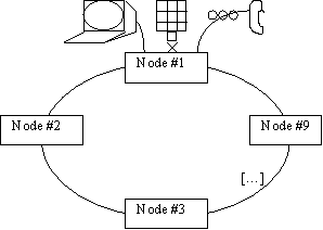
A ring network, as illustrated in Figure 1, was implemented. A total of nine nodes has been interconnected through point-to-point links using laser transmitters and PIN-detectors at the receivers. An addressing keypad is used to route the voice channel to the desired destination node. Over the voice channel a data link can then easily be established through a pair of modems, one at each end.
Figure 1 - Ring network architecture with nine nodes. Node features include voice communication, addressing and possibility for (low-baud) digital data transmission.
The architecture at each node involves a number of functional units, as depicted in Figure 2. The optical signal is detected and amplified in a moderate sensitivity receiver, followed by a processing stage including some filtering and demodulation facilities. The digital outputs are then fed into temporisation and digital processing circuits.
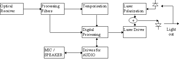
Figure 2 - Block diagram of main control/communication functions in a node.
Audio and data communication drivers are connected to the digital processing unit. A serial output with frequency multiplexed data and control information is driven into a laser which converts it to a 670 nm collimated beam pointed to the next node. A feedback control system ensures that the laser power is kept at a constant and safe average level. This is an important feature as low-cost lasers don’t normally include thermal stabilisation hardware, such as a thermo-electric cooler.
The laser used as a transmitter was the Sony SLD1122VS with a maximum output power of 5 mW in the red emission band (
l=670 nm). The detectors for the receiver were supplied by Siemens. The PIN detector SFH217 has a maximum responsivity of 0.62 A/W (quantum efficiency h=0.89 @ 850 nm and h=0.7 @ 670 nm). At the laser output, a spherical collimating lens was included for minimum beam aperture. The assembled boards were then put at different positions over the laboratory and communication tests have been successfully performed.An analytical model for the operation of the system was developed in such a way that simple estimates of performance could be assessed. Thus, limits in distance range as well as transmission speed could be calculated. The model, still in development, relies on some basic assumptions. The received beam is assumed to be completely subtended by the focusing optics and also these optics are believed to deliver all the power to the active area of the PIN photodiode [1].
Due to high absorption in the atmosphere, less significant effects on the transmitted pulses (under these circumstances) like dispersion and non-linear Kerr effect have been neglected. A FET high-impedance amplifier was considered as the first amplification stage at the optical front-end. Then, Gaussian statistics were assumed for the noise affecting the digital symbol decision circuit. As a consequence of considering low-distance and low-dispersion, intersymbol-interference and telegraphic distortion at the decision stage were also neglected.
The total optical power incident at the receiver for binary symbol iÎ {0,1} is given by
![]() (1)
(1)
where Ptx is the optical power at the laser transmitter output,
a is the air optical attenuation coefficient and L is the Tx-Rx distance of the particular link. The average electric current at the decision instant referred to the FET input is given by ![]() (2)
(2)
A certain amount Pr of residual power due to sun light or artificial illumination is considered. Rs is the detector responsivity and id takes into account its dark current. The noise is mainly due to the electric receiver thermal effects and quantum noise, arising from the quantum nature of light (photons).
![]() (3)
(3)
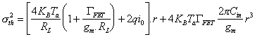
The first term is symbol-independent, but the second changes with the received power, thus with the symbol as amplitude modulation was used. The high-frequency noise is filtered by an electric low-pass filter with an equivalent bandwidth equal to the binary data rate r. The total thermal noise variance due to the FET and the polarisation resistor RL, has variance [2]
 (4)
(4)
where KB is the Boltzmann constant, Ta is the operating temperature, gm and
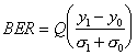
GFET are, respectively, the FET transconductance gain and the noise factor, q is the electron charge, Cin is the resulting input capacitance from the PIN and the gate of the FET and finally the current i0 is the result ofUnder Gaussian statistics, as stated above, the bit error rate (BER) is then easily calculated after the signal to noise ratio, according to the following expression [4],
 (5)
(5)
The Q-integral function is well known and can, without significant loss of accuracy, be approximated by the following
![]() (6)
(6)
In the calculations, a temperature of 300 K was considered. At the laser, a symbol one is codified by a 5 mW power level and a zero by 0.4 mW, to limit the laser chirp and maximise commutation speed. The optical power loss was 20 dB/km. The detector dark current is 3 nA and the residual optical power equals 0.2 mW. The electrical front-end is characterised by gm=40 mS, GFET=1.78, Cin=1 nF and RL=50 W.
Under the conditions above, calculations were performed to study the BER dependence on the link distance, for fixed baud rate values between 40 Mb/s and 360 Mb/s. Results are shown on Figure 3.
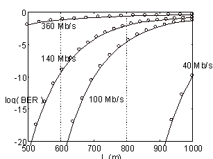
Figure 3 - BER variation with transmission range, for baud rates of 40, 100, 140 and 360 Mb/s.
Referring to the standard performance limit of BER=10-9, one may conclude that a 40 Mb/s link can be established for as much as 1000 m without reaching that limit. For rates of 100 Mb/s and 140 Mb/s, respectively, the maxim ranges are at approximately 700 m and 600 m. Less than 500 m can be covered by a 360 Mb/s system, as an error rate of 10-2 is observed for this value of L.
Now looking at the maximum baud rates attainable for fixed distances, a last set of calculations was realised with results as shown in Figure 4.
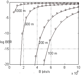
Figure 4 - BER variation with baud rate for transmission ranges of 100, 200, 500 and 1000m.
A 100 m system is then capable of supporting data channels up to 650 Mb/s. As distance increases, the maximum speed is naturally reduced. Thus, for L=200 m the maximum speed is now a little more than 450 Mb/s. For 500 m the limit is 200 Mb/s and for 1000 m it will stand below 50 Mb/s.
An experimental system has been designed and realised enabling, in its preliminary form, voice traffic to be transported over limited indoor distances. Then, well established analysis models, used in the context of fiberoptic communications, were adapted to describe the actual characteristics of our network configuration. The calculations realised with this model then showed that high distances could be achieved provided that good beam quality is guarantied. This means low divergence, basically. Also, problems with natural phenomena like rain or fog, which could limit the distance and/or transmission quality in open air systems, will not affect their indoor counterparts proposed in this paper. Neither will acoustic or electrical noise affect the network behaviour, unless very bad electric power sources are used. The transmission path itself is inherently highly insensitive to these aspects - due to its optical characteristics.
A maximum range of 700 m for a 140 Mb/s is a very good forecast for the performance of such a system, namely if compared with present electrical local area networks, like Ethernet, working at 10 Mb/s and hardly reaching more than 500 m via copper coaxial cable. Moreover, the price of the transmission path in copper-cabled systems is proportional to L, whereas our proposal requires the cheapest transmission path there is - just air.
Future work will be directed towards the digital version, optimising both the receiver and transmitter optics and developing compact, robust and easily installable units for pilot field installations. Also, alternative optoelectronic components will be tried in order to maximise the quality/price ratio and the universe of possible industry applications.
References:
[1] A. Billings, Optics, Optoelectronics and Photonics, Ed. Prentice Hall, 1993
[2] R. Smith and S. Personick, "Receiver Design for Optical Communication Systems," in Topics in Applied Physics, Vol.39, Semiconductor Devices for Optical Communications, Ed. H. Kressel, New York: Springer, 1980, pp. 89-160.
[3] S. Personick, "Receiver Design for Digital Fiber Optic Communication Systems I, " Bell Syst. Tech. J., vol.52, No.6, JUL-AUG/73, pp. 843-874
[4] G. Keiser, Optical Fiber Communications, Second Edition, Ed. McGraw-Hill, 1991