Research of the Optical Communications Groups at University of Aveiro and Institute of Telecommunications - Aveiro Pole
P.Tavares, O.Frazão, L.Ribeiro*, J.F.da Rocha, P.Monteiro,
A.Teixeira, M.Lima, P.André, J.L.Pinto, A.Pereira
Departamento de Electrónica e Telecomunicações, Universidade de Aveiro,
Campus Universitário de Santiago, 3800 Aveiro, Portugal, Tel. +351 34 370900; Fax. +351 34 377901
Dept. of Industrial Electronics, University of Minho
4810 Guimarães, Portugal, Tel. +351 53 510190, Fax +351 53 510189, botelho.ribeiro@dei.uminho.pt
Instituto de Telecomunicações, Universidade de Aveiro,
Campus Universitário de Santiago, 3800 Aveiro, Portugal, Tel. +351 34 377900, Fax. +351 34 377901
ABSTRACT
This paper resumes the research activities in optical communications systems that were performed in Portugal in the last three years. Those activities take place in the Aveiro pole of the "Instituto de Telecomunicações" and the Department of Electronics and Telecommunications of the Aveiro University. Several activities like clock recovery systems both electrical and all optical, equalisers and optical receivers and simulation work on WDM are presented.
- CLOCK RECOVERY UNIT
A clock recovery circuit (CRC), to integrate the receiver unit of a 20 Gsymbol/s optical system, using data formats with no power at the data rate (Binary NRZ and 4-level) was performed. The amplitude of the input signal was 600 mVpp, and was expected an amplitude of approximately 250 mVpp and a jitter inferior to 0.025 UI RMS for the recovered clock signal.
Clock recovery circuits can be classified into two groups: open-loop structures and closed-loop or adaptive structures. Although the adaptive approach is preferable, since its phase-lock principle has inherent automatic frequency control capabilities, at very high bit rates the technology needed for a good design and performance of such circuits is not completely mature, and the open-loop solution is preferable [1].
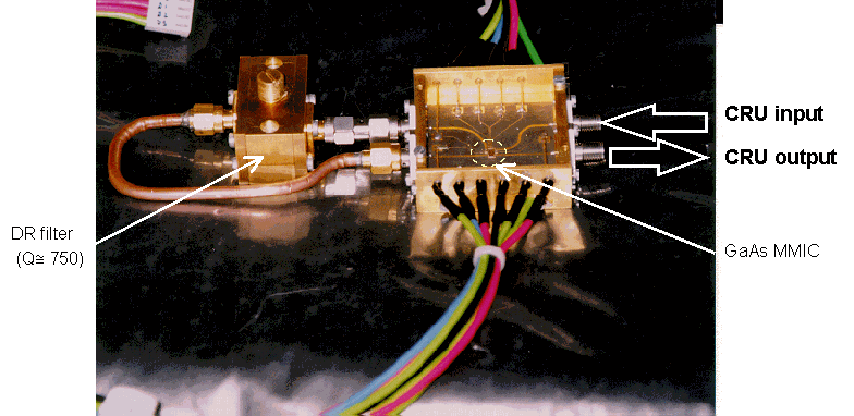
The built open-loop CRU includes a prefilter, a nonlinear circuit (NLC), a high quality factor (Q) bandpass filter and a tuned amplifier (see block diagram in fig.1). The prefilter is intended to reshape the incoming signal, in order to reduce the recovered clock jitter. A discrete frequency component at the data rate is generated using a nonlinear circuit. This NLC is an unbalanced square nonlinearity, since such structure is achieved with very simple circuits, and there is only negligible degradation in performance when compared to a balanced nonlinearity, as concluded by Matos et al [2]. The high-Q bandpass filter is intended to reduce the noise level associated to the produced discrete component, and at the considered data rate it is implemented using a dielectric resonator (DR) with a quality factor of approximately 750. Finally, the tuned amplifier has three main purposes: to provide the required signal levels, to reduce the degradation caused by the out of band spurious modes of the non-ideal high-Q bandpass filter and also to isolate the CRU from the subsequent units.
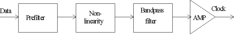
Fig. 1. Block diagram of an open-loop clock recovery unit.
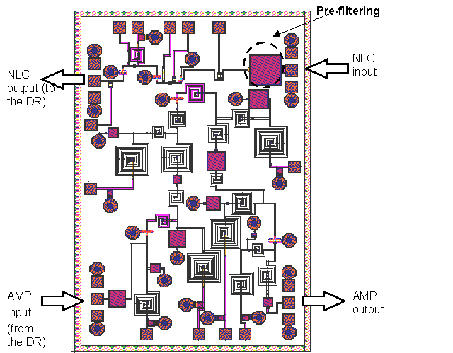
The NLC and the tuned amplifier were integrated in the same GaAs monolithic microwave integrated circuit (MMIC), in order to improve the reliability, performance and to reduce the size and the cost. The circuit has been fabricated at the PML foundry using the D02AH process, which uses 0.2 m
m gate length pseudomorphic HEMTs (high-electron-mobility transistors). The nonlinearity input stage performs the necessary signal formatting to reduce the jitter of the recovered clock, avoiding the use of additional pre-filtering. Fig. 2 a) presents the circuit mask submitted to the Foundry. The MMIC was mounted on a carrier and bond wires were used to connect it to the external circuits. In fig. 2.b) is presented the assembled circuit prototype.
|
|
|
Fig. 2. a) Mask of the MMIC (prefilter, NLC and tuned amplifier) submitted to the Foundry.
b) Assembled circuit prototype
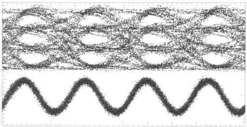
Fig. 3 presents the eye-diagrams of the recovered clock signals (bottom) and the input waveforms (up). These input wave forms are 19.90656 Gsymb/s (2*STM-64) PRBS of length 231-1 symbols and amplitude 600 mVpp, with two different line codings, Binary NRZ (Fig. 3) and 4-level (Fig. 3). T
Fig. 3.
he measured amplitude and jitter of the clock signal are respectively 200 mVpp and 0.010 UI RMS for the NRZ case, and 140 mVpp and 0.018 UI RMS for the 4-level case, thus satisfying the proposed specifications.
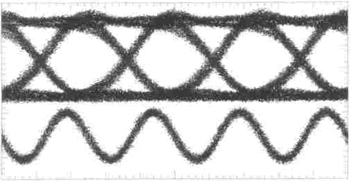
a) |
b) |
Fig. 3. Measured eye-diagrams at the input and output of the clock recovery unit considering
two different line codings. a) Binary NRZ. b) Multilevel (4-level)
SIMULATION WORK ON WDM
Major changes are occurring in telecommunications. User requirements are shifting towards new services, such as multimedia communications, high definition image transmission, high volume file transfer and others. Due to the high rates involved, such networks will use optical fibre as the transmission medium. It has been widely recognised that a network to provide an adequate level of services will have to provide multiple concurrent connectivity channels between the nodes. This can be accomplished in an optical network through the use of wavelength division multiplexing (WDM), where a different wavelength is allocated to each channel. A large variety of WDM network topologies has been proposed. They employ tuneable transmitter and/or receiver at the nodes. In that way the logical network topology becomes independent of the physical network topology, as long as all the nodes have access to all wavelengths.
In the DAWN project it is proposed a new WDM network topology which features the dynamic allocation of wavelengths. This network topology is based on the use of a Reflective Semiconductor Optical Amplifier (RSOA).
In the proposed topology, the principal components of a transmitter at each node are a RSOA and a tuneable optical filter. The node receives a signal comprising a comb of reference wavelengths and selects one of the wavelengths by appropriately setting the optical filter. The received signal travels along the RSOA where it is amplified, modulated and reflected back to the network. Besides providing gain, this simple scheme has the advantage of facilitating wavelength monitoring and control at the controlling node. At the receiver, by appropriate filtering of the received signal, the data is separated from the signalling information. A control channel is provided by adopting subcarrier multiplexing techniques [3]. The nodes are informed which wavelength is being used to carry the incoming message.
The great objective of the project is to develop a demonstrator consisting of four nodes (three user nodes and a controlling node), connected using a passive star topology. The demonstrator will operate in the 1550 nm region and will support 1 Gbit/s data transmission, using direct detection.
ELECTRICAL ADJUSTABLE EQUALIZER
An electrical adjustable equalizer was developed for very high bit rate optical communications systems using the standard single mode fibre (SMF) and based on dispersion supported transmission (DST) [4].
The equaliser was constructed in the framework of the European Community ACTS project SPEED ("Superhighway by Photonically and Electronically Enhanced Digital Transmission ").The main objective of this project is to demonstrate the feasibility of very high bitrate (20 Gbit/s and 40 Gbit/s) optical transmission systems in the transit network, using the electrical time division multiplexing approach.
Figure 4 shows the photograph of the DST equaliser and the control and bias circuits. The equalizer was designed using a GaAs monolithic technology and it has the main advantages to be electrically adjustable, a good input and output impedance match and also a small size.
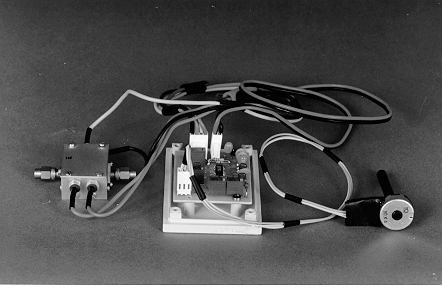
Fig. 4 -Photograph of the DST equalizer with control and bias circuits.
By using the electrical equalizer and the DST technique it is possible to transmit 20 Gbit/s, 40 Km, at standard single mode fibre without regenerating repeaters [4]. The achieved product bitrate´
distance is well beyond the limit due to the chromatic dispersion.
POST-DETECTION RECEIVER FILTER
The post-detection receiver filter has the function to reshape the received signal in order to produce well defined pulse shape with low noise, low intersymbol interference and low telegraph distortion at the input of the decision circuit. A well designed post-detection filter, effecting appropriate pulse shaping, can improve significantly the performance of the optical system. However, there are constraints in filter design: it must be easily fabricated, insensitive to manufacturing tolerances, have a reasonable physical size and must also easily integrate with the other optical receiver components.
Different microwave filter design strategies were investigated to be used at receiver units developed for the optical communication system demonstrators of the European Community projects ACTS ("Advanced Communications Technologies and Services"), namely the UPGRADE ("High Bitrate 1300nm Upgrade of the European Standard Single-Mode Fibre Network") and ESTHER ("Exploitation of Soliton Transmission Highways in the European Ring"). Both projects have the principal objectives to demonstrated in field trials and with real traffic the advantages of the return to zero (RZ) transmission systems to upgrade the present infrastructure and/or development new high capacity transport networks. The main difference between the two projects is the wavelength operation, the UPGRADE project develops optical systems for long haul and high bit rates at the second optical window and the ESTHER project develops the systems at the third optical window.
Fig. 5 shows an example of a passive post-detection filter designed for a 10 Gbit/s RZ optical receiver unit. This passive filter is based on a step impedance microstrip distributed structure and it has the advantages of simplicity and low-cost production. In spite of the good results achieved by using these filters [5, 6], it is impossible to adjust their response for different system operating conditions and therefore they must be carefully designed for each particular system.
In order to provide post-detection filters with electrical tunability there were investigated active filter structures [5, 7, 8]. Figure 6 shows an example of an active filter implement in monolithic technology for 10 Gbit/s optical soliton system. This filter exhibits a good input and output impedance match to avoid the performance degradation due to the back reflections and also a small physical size (2´
1.5´
0.1 mm3) to be easily integrated with the other receiver components.
|
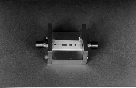
Fig. 5 Microstrip filter prototype mounted in a test carrier.
|
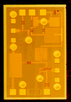
Fig. 6 Photomicrograph of an adjustable post-detection filter with active impedance matching for optical soliton communication systems.
|
SIMULATION WORK IN DST
This project is based on the Dispersion Supported Transmission (DST) accommodation scheme already standardized by the ITU-T recommendation G.691. This scheme is based on the electronic accommodation of the fiber dispersion by equalization.
Due to the second order dispersion in standard Single-Mode Fiber (SMF), the transmission of 20Gbit/s binary Non-return to Zero (NRZ) signals, without dispersion compensation, is limited to about 20km [9]. Dispersion Supported Transmission (DST) [10] overcomes the dispersion limit. This scheme makes use of direct modulation of the LASER and a simple equalization scheme [11]. Further improvements can be obtained by using DST with multi-level coding [12,13]. However, to achieve the benefits of this technique, receiver equalizer and laser must be appropriately optimized.
The configuration of this kind of systems is similar to any other case, and is presented in Figure 7 for a four-level 40Gbit/s case.
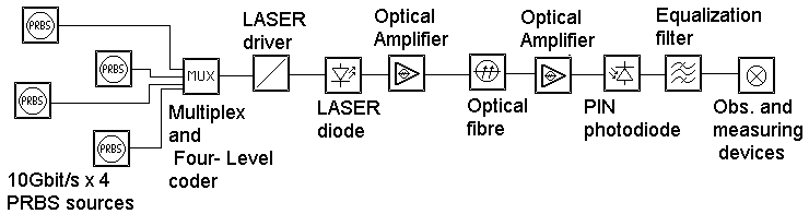
Fig. 7 Simulations set-up for the four level DST 40Gbit/s 46.2 km system
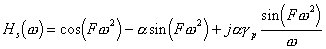
A DST system is based in the high-pass characteristic of the detected signal, that results from the frequency modulation induced by direct modulation of a diode LASER and the low-pass characteristic of the SMF. The resulting characteristic can be easily equalized for some system parameters (LASER FM efficiency, EFM, and SMF parameters).
The Small Signal Transfer Function (SSTF) of a DST system without any equalization can be written has follows [14]:
 (1)
(1)
where a
is the LASER line-width enhancement factor, g
p is the small signal decay rate for the photon population:
In these expressions D is the fiber dispersion parameter, L is the length, S0 is the photon density at bias point, t
p is the photon lifetime and e
is the non-linear gain compression factor.
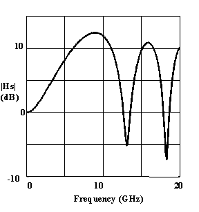
In Figure 8a), it can be found a graphical representation of this transfer function for a particular system.
|
|
|
|
Figure 8a) Modulus of the uncompensated system response for a
=2.95 and e
=3.8E-23m3 |
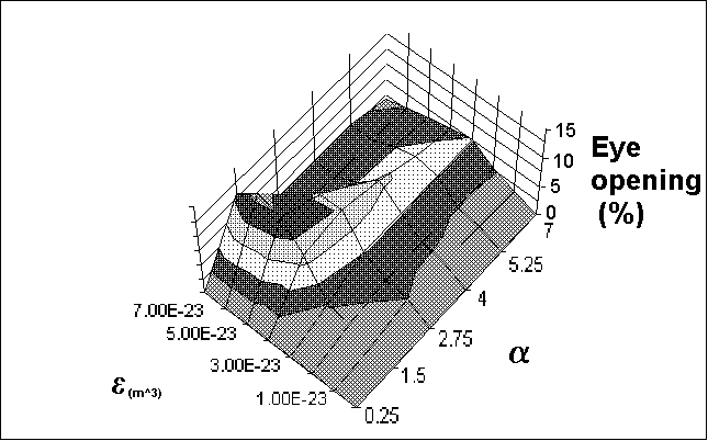
b) Eye opening as a function of a
and e
when the LASER noise is considered |
The parameters that seem suitable of optimization since are simultaneously related to the FM efficiency (EFM) and to the SSTF are the line-width enhancement factor (a
) and the NLGC (e
).
Figure 8b) shows an evaluation of the system performance based on the change of the referred parameters of the laser [15]. The performance assessment was made based on an average of the three eyes opening. As it can be observed there a particular point where the performance of the system is optimum. In any case all other parameters are optimized for each obtained point.
Other step needed for the best performance of the system is to get the best optimization scheme possible. The work led us to the use of a pole-zero configuration of the receiver equalizer. The need for this flexibility comes from the fact that there are several types of laser that can be used for transmitting DST.
The pole frequency can be obtained simply by [16], but in practice there must be made some little tuning. It was then suggested another formulation [17]:
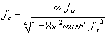 , (2)
, (2)
 ,
, 
Where m is a power index (normally set to one), EFM is the FM efficiency, I0,th are the bias and the threshold current of the laser respectively and the remaining parameters were already defined.
With respect to the zero, this is only needed in some cases, as shown in Figure 9. The flat zone represents the range where the zero is almost not noticed.
This work has been partly supported by the Portuguese program PRAXIS XXI and the European Commission in the project AC049 "SPEED".
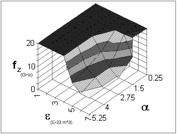
Fig. 9 Equalizer zero frequency as a function of the a
and the e
of the LASER
for optimized eyes opening at the system output
ASSESSMENT OF EDFA IMPACT ON IM-DD OPTICAL COMMUNICATION SYSTEMS
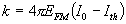
This project intended to assess the actual impact of optical pre-amplification, e.g. by an EDFA, on the performance of optical receivers. The more accurate existing methodologies involved the use of Moment Generating Functions in bounds for the bit-error rate. The challenge was then to develop new or the same bounds with a new and trusted Moment Generating Function taking into account the noise sources and stochastic processes ocurring in the optical domain, due to amplification. As a consequence, an experimental prototype was actually built from scratch, including the control and interface electronics as well as software. The project was partially sponsored by JNICT-Portuguese Office for Scientific & Technological Research, and the European Community under the RACE project (EU-R2001).
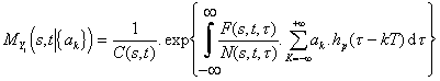
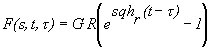
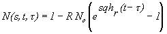
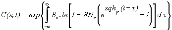
The fotocurrent of a detector was analitically derived yielding [?],e sem ruído eléctrico aditivo.
Assim, para um bit de informação isolado, codificado por um impulso de potência hp(t), a FGM da corrente detectada é dada por
 (1)
(1)
de saída filtrada por hr(t)
Considerando a interferência entre símbolos vizinhos, a FGM deve ser generalizada por forma a incorporar contribuições de outros bits além do bit de decisão a0 para a corrente Y=y(t).
Com base na independência dos bits de informação ak, pode calcular-se a esperança da FGM para o símbolo "0"
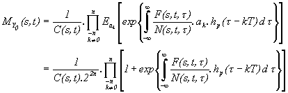 (2)
(2)
Procedendo de forma análoga, obtém-se a FGM condicionada para o símbolo "1"
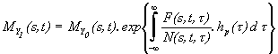 (3)
(3)
Finalmente, contabilizamos o ruído aditivo eléctrico com variância
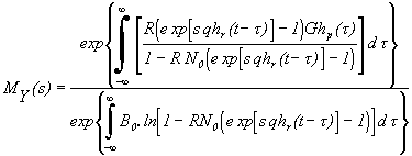
spre2. Considerando a independência estatística entre este e y(t), a FGM da variável de decisão z(t) vale
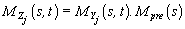 , j=0,1. (4)
Uma vez que se trata de ruído Gaussiano, tem-se
 (5)
(5)
com
 (6)
(6)
onde
 (7)
(7)
 (8)
(8)
 (9)
(9)
O novo modelo de análise de sistemas de comunicação com pré-amplificação óptica veio a ultrapassar limitações de que padeciam as primeiras tentativas de Fyath [1], [2] e Lane [3]. Estes autores propuseram certas metodologias de análise que não conseguiam descrever com rigor o comportamento estocástico da corrente de decisão. Nomeadamente, as fórmulas obtidas para a variância da corrente contradiziam os resultados amplamente confirmados de Yamamoto [4] e Personick [5]. A validação do modelo recorrerá ainda à comparação com resultados de simulação.
A. Acordo com expressões de Yamamoto
Considerando um filtro arbitrário e partindo das propriedades da FGM, por derivação da eq. (1), obtém-se a média e a variância do sinal de saída
As componentes
s2s, s2sp, s2s_sp, s2sp_sp representam respectivamente o ruído quântico de sinal, ruído quântico da EEA, a potência óptica média, foi desprezado por Yamamoto [7], mas inclui-se aqui para o caso geral.
B. Acordo com resultados de simulação
Realizaram-se estudos quantitativos para comparar previsões do desempenho de um sistema dado com resultados de simulação de Monte-Carlo.
Para isso foram utilizados os conhecidos majorantes de Chernoff (MC) e de Chernoff modificado (MCM) [6] baseados na função geradora de momentos, além de uma aproximação Gaussiana.
V. Construção de um AFiDE
Foi projectado e construído um protótipo de um AFiDE. O módulo principal compõe-se de uma parte óptica, onde ocorre fisicamente o processo de amplificação do sinal óptico, e uma parte electrónica destinada a controlar a primeira e a obter, ao mesmo tempo, dados quantitativos sobre o estado de funcionamento do dispositivo.
Fisicamente, o módulo é constituído por um diodo-laser semicondutor de Pmax=50 mW, a emitir em lb=980 nm, acoplado a um troço activo de 40 m de fibra dopada de érbio. Este esquema básico, sem quaisquer filtros ou isoladores ópticos, permite uma grande versatilidade na
utilização do módulo em diferentes aplicações. Para o uso como amplificador óptico simples com bombagem progressiva, filtragem da potência da bomba residual na saída e monitorização de potência foi também construído um módulo auxiliar contendo os restantes componentes necessários.
O módulo é alimentado directamente a partir da rede de 220V. O utilizador dispõe de um painel de comando, a partir do qual pode definir parâmetros de funcionamento e obter informações do estado do sistema (alarmes, indicadores e medidas) através de uma série de LEDs e de um mostrador de cristais líquidos. O teclado permite comutar entre os modos manual e remoto, no qual o AFiDE atende comandos do exterior via porta série.
A. Montagem óptica
Grande parte do módulo principal foi realizada nos laboratórios da "SEL-Alcatel Forschungszentrum" (Estugarda-Alemanha). É no módulo principal que se dá efectivamente a amplificação do sinal. No caso presente, pretendeu-se construir um AFiDE de onda progressiva para funcionar como pré-amplificador óptico. Para isso o módulo auxiliar realiza a rejeição da bombagem residual na saída e alguma filtragem da EEA fora da zona de interesse para sinal. Além disso faz também amostragem da potência de entrada e saída para monitorização.
Na Error! Reference source not found. encontra-se o esquema da montagem óptica do módulo principal. Este módulo inclui um laser de bombagem (Lasertron-QLM9S470 50 mW / 980 nm), o misturador óptico (MO), a secção activa (FDE), as juntas de fusão necessárias ao acoplamento dos componentes e os conectores de entrada e saída.
Montagem electrónica
C. Caracterização óptica do AFiDE
Os resultados que se apresentam foram obtidos com um analisador de espectros óptico. Fez-se um varrimento da potência de bombagem entre 25 mW e 63 mW. Para cada valor ao longo desta gama, a potência de sinal Ps(0) foi variada em passos de 5 dB desde -40 dBm até -5 dBm.
References:
[1] J. N. Matos, A. Gameiro, P. Monteiro, J. F. da Rocha, "Bit synchronization in multigigabit receivers", SPIE Proceedings Series, vol. 1974, pp. 148-158, April 1993.
[2] J. N. Matos, A. Gameiro, P. Monteiro, J. F. da Rocha, "Dielectric resonator based synchronizer for multigigabit optical communications", Proceedings of 23rd European Microwave Conference, pp. 941-943, 1993.
[3] S. F. Su, A. R. Bugos, V. Lanzisera, and R. Olshansky, "Demonstration of a multiple-access WDM network with subcarrier multiplexed control channels", IEEE Photonics Letters, vol.6, n.3, March 1994.
[4] Paulo P. Monteiro, Mário J. Lima, António L. Teixeira, José Ferreira da Rocha, "An Electrically Adjustable Equalizer for Very High Bit Rate Transmission Systems based on Dispersion Supported Transmission", ICECS'98, 5th IEEE International Conference on Electronics, Circuits and Systems, September 1998, pp. 193-196.
[5] P.M. Monteiro, A. Borjak, F. da Rocha, J.J. O´Reilly, I. Darwazeh, "Microwave Pulse Shaping Filters for Multigigabit Optical Systems"; NOC´96 -European Conference on Networks & Optical Communications, Junho de 1996, na Alemanha, pp. 232-239
[6] P. Monteiro; L.R. Watkins; J.J. O'Reilly; J.R.F. da Rocha; "Pulse Shaping Microstrip Filters for 10 and 15 Gbit/s Optical Receivers". SPIE Proceedings, Vol. 1784,1992 Boston, pp.12-18.
[7] Paulo P. Monteiro, Pedro L. Antunes, Mário J. Lima, José F. da Rocha, "Adjustable Pulse Shaping Filter with Active Impedance Matching for Optical Soliton Communication Systems", GAAS'98 conference proceedings, Amsterdam 6-8 October 1998.
[8] P. Monteiro, A. Borjak, F. da Rocha, J.J. O´Reilly, I. Darwazeh "10 Gbit/s Pulse Shaping Distributed-Based Transversal Filter Front-end for Optical Soliton Receivers", IEEE Microwave and Guided Wave Letters, Vol. 8, Nº 1, Janeiro 1998, pp. 4-6
[9] W.S.Lee, G.A. Pettitt, J. Wakefield, B.L. Patel, A.Hadjifotiou: "Optically amplified high capacity transmission at 20Gbit/s by TDM", Electron. Lett., 30, 1994, pp. 584-586.
[10] B. Wedding, "A new method for optical transmission beyond the dispersion limit", Electron. Lett., 28, 1992, 14, pp. 1298-1300.
[11] B. Wedding, K. Koeffers, B. Franz, D Mathooasing, Ch Kazmierski, P. Monteiro, J. Matos, " Dispersion-Supported transmission of 20Gbit/s over 53km standard singlemode fibre", Electron. Lett., 31, 1995, 7, pp.566-568.
[12] X. Gu, L.C. Blank, " 10Gbit/s unrepeatered three level optical transmission over 100km standard fibre", Electron. Lett., 29, 1995, 29, pp. 2209-2211.
[13] B. Wedding, W. Pöhlmann, B. Franz, H. Geupel, " Multi-level dispersion supported transmission at 20Gbit/s over 46km installed standard single mode fibre", ECOC'96 proceedings, 1996, pp. 1.91-1.94.
[14] J. Wang, K. Peterman, "Small signal analysis for dispersive optical fiber communication systems", J. of Lightwave Tech., 10, 1993, pp. 812-813
[15] António L.J. Teixeira, Rui F. S. Ribeiro, José R. F. da Rocha, Laser optimisation for multi-level Dispersion Supported Transmission systems", LEOS 97, San Francisco, Califórnia, 7-13 November 1997
[16] António L.J. Teixeira, Rui F. S. Ribeiro, José R. F. da Rocha, "Equaliser optimisation for multi-level Dispersion Supported Transmission systems", TSR 97, University College of London, London, UK, 21-22 of July 1997
[17] António L.J. Teixeira, R F S Ribeiro, J R F da Rocha, "Effects of non-ideal frequency modulation on multilevel dispersion supported transmission systems", Conf. proceedings No. 451, pp.54-56, 6th conference on telecommunications, Edinbourgh, 29 March to 1 April 1998